Search results
Search for "band diagram" in Full Text gives 29 result(s) in Beilstein Journal of Nanotechnology.
Observation of multiple bulk bound states in the continuum modes in a photonic crystal cavity
Beilstein J. Nanotechnol. 2023, 14, 544–551, doi:10.3762/bjnano.14.45

- reflective boundary around the BIC cavity [29][30], a bandgap mirror and transition area surrounding the designed BIC cavity are proposed. We numerically evaluate the bulk band diagram of the corresponding infinite BIC structure as well as the multiple quantized bulk mode profiles of the finite-size BIC
- cell. (a) Schematic of a unit cell consisting of an AlGaAs nanoblock on a sapphire substrate. The side length and the height of the nanoblock are w and h, respectively. The period of the unit is p. (b) Band diagram related to the MD BIC mode. The electric field distribution for the mode at the Г point
- bandgap heterostructure, respectively. Na, Nb, Pa = p, and Pb are the number of nanoblocks and lattice periods in regions A and B, respectively. Inset: the transition region at the interface between the two regions. (b) Band diagram of the structures in regions A and B. (c) The momentum distribution of


High–low Kelvin probe force spectroscopy for measuring the interface state density
Beilstein J. Nanotechnol. 2023, 14, 175–189, doi:10.3762/bjnano.14.18

- high-resolution nanoscale measurements of impurity concentration and defect level distributions at the surfaces and interfaces of various semiconductor materials and devices. (a) Schematic of the metal tip–gap–semiconductor sample. (b) Energy band diagram of the metal–gap–semiconductor sample. Emission


Photoelectrochemical water oxidation over TiO2 nanotubes modified with MoS2 and g-C3N4
Beilstein J. Nanotechnol. 2022, 13, 1541–1550, doi:10.3762/bjnano.13.127

- results previously published in [58]. Figure 7 presents the energy band diagram structure of the MoS2/TNAs and g-C3N4/TNAs heterojunctions based on the DRS and Mott–Schottky analysis results, which are summarized in Table 1. It is easily observed from Figure 7 that the heterostructures formed upon
- optical properties of as-synthesized materials through DRS spectra (a) and Tauc plots (b). EIS spectra (a), Mott–Schottky plots of pristine materials (b) and heterostructures (c). LSV plots (a), Tafel slopes (b), and photo-response (c) of the materials. Proposed band diagram of MoS2/TNAs (a) and g-C3N4


The effect of metal surface nanomorphology on the output performance of a TENG
Beilstein J. Nanotechnol. 2022, 13, 298–312, doi:10.3762/bjnano.13.25

- –semiconductor and semiconductor–metal contact pairs [14][15]. A semiconductor–metal contact can be described by the band diagram shown in Figure 1. The frictional electrical properties of materials depend on their work functions and Fermi levels [16][17]. The intermediate state in the bandgap can reduce the


A Au/CuNiCoS4/p-Si photodiode: electrical and morphological characterization
Beilstein J. Nanotechnol. 2021, 12, 984–994, doi:10.3762/bjnano.12.74

- in a high-vacuum coating unit. Thus, the Au/CuNiCoS4/p-Si photodiode device was fabricated. The schematic illustration of the photodiode device and a band diagram of the junctions, with bandgaps and energy levels is shown in Figure 1. The device has a barrier at the interfacial layer between Au and p
- illustration and (b) band diagram of the fabricated Au/CuNiCoS4/p-Si photodiode. (a) XRD pattern and crystal structure model, (b) TEM image, (c) HR-TEM interplanar spacing image, (d) FE-SEM image and (e) EDS pattern of the CuNiCoS4 nanocrystals. (a) Absorbance spectroscopy graph (inset figure: diffuse


Impact of GaAs(100) surface preparation on EQE of AZO/Al2O3/p-GaAs photovoltaic structures
Beilstein J. Nanotechnol. 2021, 12, 578–592, doi:10.3762/bjnano.12.48

- the Al concentration is increased (5–6%); however, it is still quite low and occupies a relatively wide area. Thus it was not included in the energy band diagram (Figure 7) as a separate dielectric layer. While constructing the diagram for AZO we adopted the following values of electron affinity χAZO
- ) of the samples of the B series. Energy band diagram of the fabricated AZO/Al2O3/p-GaAs devices. (a) EQE of sulfur-passivated samples (A series). (b) EQE of non-passivated samples (B series). I–V characteristics of the measured samples of A series (a) and B series (b). The content of O, Zn, Al, Ga


Boosting of photocatalytic hydrogen evolution via chlorine doping of polymeric carbon nitride
Beilstein J. Nanotechnol. 2021, 12, 473–484, doi:10.3762/bjnano.12.38

- the band diagram is presented in Figure 8d. The VB and CB positions to the more positive potential after chlorine doping is shifted, indicating strengthened reducibility of electrons in CB. This is one of the factors influencing the enhanced photocatalytic activity in the hydrogen evolution reaction
- ) valence band (VB) XPS spectra, and (d) band diagram of PCN and Cl-PCN. (a) Photocurrent response and (b) EIS spectra of PCN and Cl-PCN. C, N, O, and Cl atomic concentration in PCN and Cl-PCN. Chemical composition of PCN and Cl-PCN calculated from the peak-fitting procedure applied to the N 1s and C 1s


High-responsivity hybrid α-Ag2S/Si photodetector prepared by pulsed laser ablation in liquid
Beilstein J. Nanotechnol. 2020, 11, 1596–1607, doi:10.3762/bjnano.11.142

- 0.64 to 1.85 A/W at 510 nm after adding CTAB. The energy band diagram of the α-Ag2S/p-Si photodetector under illumination was constructed. The fabricated photodetectors exhibited reasonable stability after three weeks of storage under ambient conditions with a responsivity of 70% of the initial value
- . The energy band diagram under illumination of the n-Ag2S NPs/p-Si heterojunction prepared in pure Tu is shown in Figure 14. The electron affinity of Ag2S required for the band line-up construction was obtained from reported data [50]. As shown in Figure 12, the photocurrent in the photodetector came
- surfactant. The responsivity of the Ag2S/Si photodetector at 460 nm was increased by a factor of three after CTAB was added. The energy band diagram of Ag2S–Si heterojunction was constructed from optical and electrical results. The photodetectors exhibited good stability, retaining more than 70% of the


Synthesis and acetone sensing properties of ZnFe2O4/rGO gas sensors
Beilstein J. Nanotechnol. 2019, 10, 2516–2526, doi:10.3762/bjnano.10.242

- spheres of pure ZnFe2O4 and (b) of ZnFe2O4/rGO with 0.5 wt % rGO to acetone at different concentration. Response of the 0.5 wt % ZnFe2O4/rGO sensor to 10 ppm of acetone, ethanol, methanol and formaldehyde at 200 °C. Schematic of the proposed acetone sensing mechanism of ZnFe2O4/rGO. Band diagram of rGO


A carrier velocity model for electrical detection of gas molecules
Beilstein J. Nanotechnol. 2019, 10, 644–653, doi:10.3762/bjnano.10.64

- other hand, the charge transfer between GNRs and the adsorbed target molecule can change the concentration of the carriers and modulate the conductivity of the GNR. In addition, because of the atomic forces and charge transfer, molecular adsorption can lead to modification of the energy band diagram and
- interaction with the AGNR surface. The band structure of the AGNR before and after CO and NO adsorption are illustrated in Figure 5a–c. The energy band diagram of the bare ribbon shows a very small band gap, Eg = 0.085 eV, that indicates semi-metallic properties. Furthermore, it is shown that the adsorption


Sub-wavelength waveguide properties of 1D and surface-functionalized SnO2 nanostructures of various morphologies
Beilstein J. Nanotechnol. 2019, 10, 379–388, doi:10.3762/bjnano.10.37

- measurements and a band diagram is proposed. Keywords: functionalization; nanowires; photoluminescence; SnO2; sub-wavelength waveguide; Introduction The development and understanding of one-dimensional (1D) nanowire (NW) sub-wavelength waveguides is a crucial step towards on-chip routing of optical signals
- -functionalized NBs are also demonstrated. The emission from these NWs, upon excitation with a 325 nm laser, are shown to originate from the defect emission. Temperature-dependent PL studies were carried out to probe the nature of defects in these NWs. A possible band diagram for the SnO2 NWs is proposed
- this luminescence and also its source, temperature-dependent photoluminescence studies were carried out. Temperature-dependent photoluminescence and band diagram A temperature-dependent PL study was carried out to probe the detailed luminescence properties of the SnO2 NWs. Figure 8a–c shows the


Graphene-enhanced metal oxide gas sensors at room temperature: a review
Beilstein J. Nanotechnol. 2018, 9, 2832–2844, doi:10.3762/bjnano.9.264

- value after each response cycle. The band diagram of SnO2–rGO before and after the combination. An illustration of the formation of p–n heterojunctions in SnO2–rGO hybrids. Reproduced with permission from [56], copyright 2015 American Chemical Society. Representative physical models for NO2 sensing


Variation of the photoluminescence spectrum of InAs/GaAs heterostructures grown by ion-beam deposition
Beilstein J. Nanotechnol. 2018, 9, 2794–2801, doi:10.3762/bjnano.9.261

- : the top with a GaAs strain-reducing layer; the bottom with a strained buffer layer (wetting layer) [15][16][17][18][19]. Thus, the simplified energy band diagram of the active region of an InAs/GaAs heterostructure is an InAs quantum dot built into a GaAs matrix in the form of a quantum well. It
- GaAs makes it possible to change the lattice mismatches. The GaAs energy band diagram varies greatly due to the large size of Bi atoms. Emerging strains in the GaAsBi layer should have an influence on the surface density and sizes of InAs QDs and also on the photoluminescence properties of InAs/GaAs
- deep into the energy gap. This induces a change in the profiles of the valence and the conduction bands of the InAs/GaAs heterostructure. The InAs/GaAs1−xBix heterointerface forms a type-II misaligned heterojunction [60]. In accordance with the band diagram in Figure 5, the profile of the valence band


Impact of the anodization time on the photocatalytic activity of TiO2 nanotubes
Beilstein J. Nanotechnol. 2018, 9, 2628–2643, doi:10.3762/bjnano.9.244

- ) Schematic for the band diagram estimated from the measurements. a) Schematics of the experimental setup used for the PEC degradation of MB. b) UV–vis spectra for the initial MB solution and after 180 min of treatment. c) Relative MB concentration followed in situ with a 638 nm laser. d) Removal percentage


Intrinsic ultrasmall nanoscale silicon turns n-/p-type with SiO2/Si3N4-coating
Beilstein J. Nanotechnol. 2018, 9, 2255–2264, doi:10.3762/bjnano.9.210

- ultrathin Si3N4/SiO2/Si3N4: (a) physical layout shown for self-blocking p-channel FET. Schematic band diagram of such an FET shown for (b) zero and (c) negative gate bias relative to source voltage, resulting in a conductive channel by shifting the electronic Si-NWire states pinned by SiO2. Interchanging


A scanning probe microscopy study of nanostructured TiO2/poly(3-hexylthiophene) hybrid heterojunctions for photovoltaic applications
Beilstein J. Nanotechnol. 2018, 9, 2087–2096, doi:10.3762/bjnano.9.197

- between Figure 3e and Figure 3f. The origin of the contrast is therefore not to be linked to the Vcpd variations in the TiO2 surface, but rather to an inhomogeneous contribution of the grafted P3HT-COOH. Figure 4 shows a schematic representation of the band diagram of the ITO/TiO2/P3HT-COOH/tip electronic


Cyclodextrin inhibits zinc corrosion by destabilizing point defect formation in the oxide layer
Beilstein J. Nanotechnol. 2018, 9, 936–944, doi:10.3762/bjnano.9.86
- that affecting the defect chemistry of passivating films by molecular inhibitors maybe a viable strategy to control corrosion of metals. Keywords: band diagram; defect chemistry; organic corrosion inhibitors; X-ray photoelectron spectroscopy; zinc corrosion; Introduction Organic corrosion inhibitors
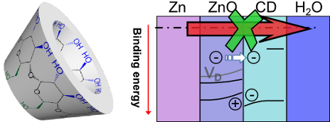
- likely that β-CD accepts the charge via the hydroxy groups. The charge dislocation explains the observed energy level shift in photoemission experiments, closely resembling band bending. From the derived band diagram, charge dislocation could also take place via holes. Due the lower mobility of holes
- ). Band diagram of the β-CD/ZnO interface constructed from photoemission experiments, with energy levels in electronvolts. XPS and He II UPS sensitivity areas are distinguished by the different color intensity, the given thickness values are rough estimates only. The upward energy level shift in ZnO is a


Impact of contact resistance on the electrical properties of MoS2 transistors at practical operating temperatures
Beilstein J. Nanotechnol. 2017, 8, 254–263, doi:10.3762/bjnano.8.28

- voltage VFB,id can be expressed as: where ψth is the downward (negative) band bending at the threshold (as illustrated in the band diagram (iii) of Figure 3c, and Ns(ψth) is the electron density in the channel at ψth where is the Debye length. The band bending ψth can be evaluated assuming that the


Nanocrystalline TiO2/SnO2 heterostructures for gas sensing
Beilstein J. Nanotechnol. 2017, 8, 108–122, doi:10.3762/bjnano.8.12

- dependence on the partial pressure of H2. In the case of 90 mol % SnO2/10 mol % TiO2, O2− and O− ions are adsorbed and the ratio of O−/O2− increases with temperature. Schematics illustrating the beneficial action of n–n heterojunctions for the sensitization of the gas sensor. (a) Electronic band diagram of


Charge injection and transport properties of an organic light-emitting diode
Beilstein J. Nanotechnol. 2016, 7, 47–52, doi:10.3762/bjnano.7.5

- efficacy (60–70 lm/W), which is the current benchmark for novel light sources [4]. Organic semiconductors have zero doping level and very low intrinsic charge density, therefore all charges in OLED device are injected from the electrodes. As a result, the energy band diagram analysis plays a key role in
- steady-state current–voltage characteristics recorded at various temperatures have been used to evaluate the activation energy of electric conductivity. Obtained results are compared with energy band diagram to identify major energy barriers limiting the current. Experimental The study of the charge
- dominates in the high-voltage region. The energy band diagram reconstruction is required for further identification of the energy barrier origin. The work function of cleaned ITO electrodes is at a level of 4.9 eV [18][19], while the Al electrode reaches only 4.2 eV [20]. The energies of the highest


Large area scanning probe microscope in ultra-high vacuum demonstrated for electrostatic force measurements on high-voltage devices
Beilstein J. Nanotechnol. 2015, 6, 2485–2497, doi:10.3762/bjnano.6.258

- expected built-in voltage. In Figure 6e a schematic band diagram shows the influence of the surface band bending as well as the characteristic energies for the n-doped SiC sample. The surface defect states are placed at energies as determined by T. Seyller [52]. DUHB and DLHB are the upper and lower Mott
- measures ΔΦ = 720 meV. Scan size: 50 × 50 μm2. a) Topography, b) dark KPFM and c) 30% laser-power illuminated (470–480 nm and a maximum power of 50 mW) KPFM images of a SiC p/n-junction. The scan size is 4 × 8 μm2. d) 100% laser- power illuminated KPFM image. e) shows a schematic band diagram of the


Current–voltage characteristics of manganite–titanite perovskite junctions
Beilstein J. Nanotechnol. 2015, 6, 1467–1484, doi:10.3762/bjnano.6.152

- current. This can be discussed according to Figure 10, where the expected simplified band diagram of the manganite–titanate junction is shown for electro-chemical equilibrium and with applied voltage in both forward and reverse directions. We disregard here all changes of the electronic structure of the
- interface. Previous studies of a PCMO–STNO junction show the rectifying character of the J–V curve can predict a p–n diode-type band diagram for this type of junction [64]. In contrast to our study, a lower doping level of Nb (y = 0.0002) was used, which leads to a more extended space charge region in the


Effects of swift heavy ion irradiation on structural, optical and photocatalytic properties of ZnO–CuO nanocomposites prepared by carbothermal evaporation method
Beilstein J. Nanotechnol. 2015, 6, 928–937, doi:10.3762/bjnano.6.96

- tests using 3 × 10¹³ ions/cm2 irradiated sample for two runs of photocatalytic degradation studies on MO dye. Schematic energy band diagram of ZnO–CuO nanocomposite showing the charge transportation processes leading to sun-light-driven photocatalytic degradation of dye. Acknowledgements The authors


Low cost, p-ZnO/n-Si, rectifying, nano heterojunction diode: Fabrication and electrical characterization
Beilstein J. Nanotechnol. 2014, 5, 2216–2221, doi:10.3762/bjnano.5.230

- . Energy band diagram and carrier transport The energy band diagram of the p-ZnO/n-Si nano heterojunction diode is depicted in Figure 4. The band gap of n-Si is 1.1 eV [9][10] and p-ZnO is 3.37 eV and the electron affinity of p-ZnO (χp) and n-Si (χn) is 4.35 eV and 4.05 eV, respectively [8]. The energy
- band diagram shows a small conduction band offset of 0.3 eV as calculated by ΔEc = q(χp − χn) and a large valance band offset 1.97 eV calculated by ΔEv = ΔEg − ΔEc. There is a diffusion of electrons from n-Si to p-ZnO and a diffusion of holes from p-ZnO to n-Si. At low, forward voltage, the current is
- used for the capacitance–voltage (C–V) measurements of the iode. XRD pattern of p-ZnO nanoparticles. (a) I–V characteristics of the diode under dark and UV illumination and (b) lnI vs V curve under dark and UV illumination. 1/C2 versus voltage curve of the nano heterojunction diode. Band diagram of a p


Electrical contacts to individual SWCNTs: A review
Beilstein J. Nanotechnol. 2014, 5, 2202–2215, doi:10.3762/bjnano.5.229

- permission from (a) [14] copyright 2000 American Physical Society, (b) [15] copyright 2005 American Chemical Society. The energy band diagram of a CNFET. a) The band bending effect at the metal–SWCNT interface for a metal with a low work function. A positive voltage bias is applied between drain–source


